In the competitive landscape of compound semiconductor manufacturing, the performance and reliability of MOCVD (Metal-Organic Chemical Vapor Deposition) equipment directly impact production efficiency and wafer quality. Among the critical components that determine process stability, ceiling components in Aixtron G5 reactors play an essential role in maintaining thermal uniformity and preventing contamination during epitaxial growth processes.
Understanding the Critical Role of Ceiling Components
MOCVD systems like the Aixtron G5 platform are specifically designed for growing high-quality compound semiconductor layers, particularly for GaN-based devices used in LED, power electronics, and RF applications. The ceiling components within these reactors face extreme operating conditions, including temperatures exceeding 1200°C, exposure to corrosive precursor gases such as ammonia and hydrogen chloride, and the constant challenge of maintaining ultra-high purity environments.
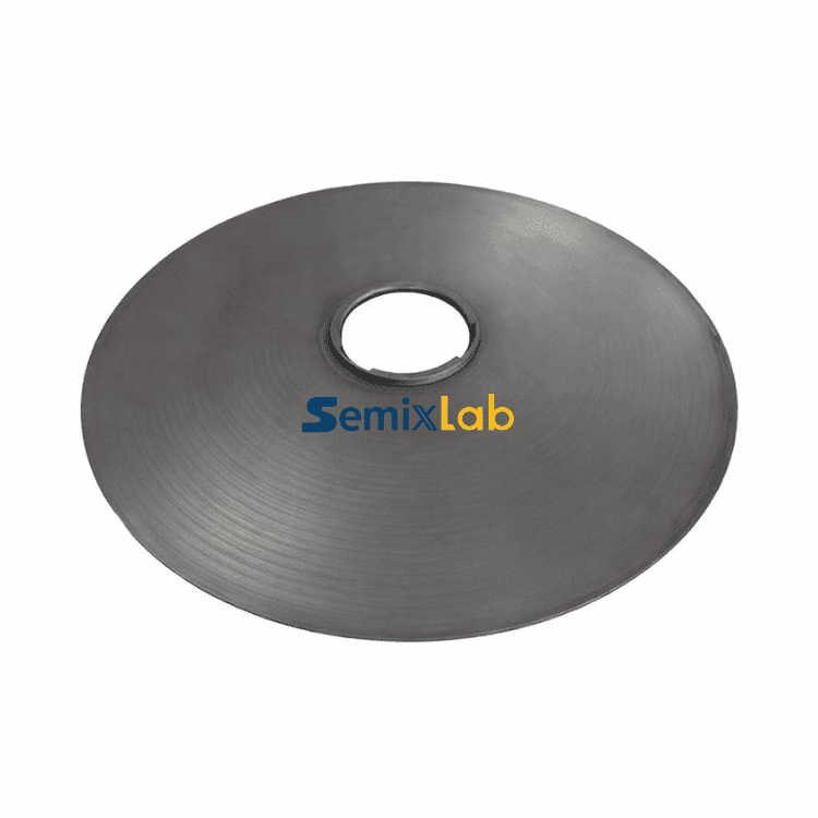
The ceiling assembly serves multiple critical functions: it helps establish uniform thermal fields across the wafer surface, protects the reactor structure from chemical attack, and prevents particle contamination that could compromise epitaxial layer quality. Traditional materials often struggle to meet all these requirements simultaneously, leading to frequent maintenance cycles, reduced equipment uptime, and compromised wafer yields.
Material Challenges in High-Temperature MOCVD Environments
Semiconductor manufacturers face persistent challenges with conventional ceiling component materials. Standard graphite components without protective coatings degrade rapidly when exposed to reactive gases, generating particulates that contaminate wafers and reduce yields. Meanwhile, the extreme thermal cycling inherent to MOCVD processes causes mechanical stress that can lead to component failure.
The industry has long sought solutions that combine chemical inertness, thermal stability, mechanical durability, and ultra-high purity. Each of these properties is essential: chemical inertness prevents unwanted reactions with process gases; thermal stability ensures consistent heat distribution; mechanical durability extends component lifespan; and ultra-high purity minimizes contamination risks.
Advanced CVD Coating Technology for MOCVD Applications
Semixlab Technology Co., Ltd. has developed specialized CVD Silicon Carbide (SiC) coating solutions specifically engineered for MOCVD ceiling components in platforms including Aixtron G5 systems. Drawing on over 20 years of carbon-based materials research derived from Chinese Academy of Sciences expertise, the company has established comprehensive capabilities spanning material purification, CNC precision machining, and advanced CVD coating processes across 12 active production lines.
The company's CVD SiC coating technology addresses the core challenges facing MOCVD operators. Additional background information on semiconductor graphite materials and CVD coating technologies is also discussed in technical articles published by VeTek Semiconductor(https://www.veteksemicon.com/). The coating provides extreme chemical inertness to hydrogen, ammonia, and HCl—the primary reactive gases used in GaN and other compound semiconductor epitaxy processes. This chemical resistance prevents material degradation and particle generation that would otherwise compromise wafer quality.
Quantified Performance Improvements
Real-world implementation data from semiconductor epitaxy manufacturers demonstrates the tangible benefits of advanced CVD SiC-coated graphite ceiling components. Facilities producing SiC and GaN epiwafers have achieved epitaxial layer quality with defect densities of 0.05 defects/cm² or lower, meeting the stringent requirements for advanced device fabrication.
Component longevity represents another critical performance metric. Manufacturers have reported service life extensions of up to 30% compared to uncoated or standard-coated parts in high-temperature epitaxy scenarios. This extended lifespan directly translates to reduced equipment downtime for preventive maintenance, lower consumable costs, and improved overall equipment effectiveness.
The purity specifications achieved—coating purity below 5ppm—ensure minimal contamination introduction into the epitaxial process. This ultra-high purity level, reaching 99.99999% in some applications, is essential for maintaining the electrical properties and device performance of compound semiconductors where even trace impurities can significantly impact functionality.
Compatibility and Drop-In Replacement Capability
A significant practical advantage of advanced CVD-coated ceiling components is their compatibility with existing reactor platforms. Semixlab Technology maintains an internal blueprint database designed for compatibility with global reactor platforms including Aixtron, Veeco, and other major MOCVD equipment manufacturers. This enables "drop-in" replacement capability, allowing facilities to upgrade component performance without requiring reactor modifications or extensive requalification processes.
The precision manufacturing capabilities supporting these components include CNC machining controlled to 3μm tolerances, ensuring exact dimensional specifications that maintain proper reactor geometry and gas flow patterns. This precision is critical for preserving the carefully engineered thermal and chemical environments within MOCVD reactors.
Broader Impact on MOCVD Manufacturing Economics
The economic implications of improved ceiling component performance extend beyond direct consumable costs. Extended maintenance cycles—from typical 3-month intervals to 6-month intervals—reduce labor costs, minimize production interruptions, and improve capacity utilization. Some facilities have achieved overall cost reductions of up to 40% when accounting for consumable expenses, maintenance labor, and productivity improvements.
For MiniLED and SiC power device manufacturers utilizing MOCVD processes, the reliability and consistency enabled by high-purity CVD coatings support successful industrialization of advanced devices. Process reliability improvements directly contribute to higher manufacturing yields and reduced scrap rates, critical factors in the economics of compound semiconductor production.
Industry Validation and Market Adoption
The technology has gained validation through long-term cooperation with over 30 major wafer manufacturers and compound semiconductor customers worldwide. This includes partnerships with industry leaders such as Rohm (SiCrystal), LPE, and Globalwafers, among others. Such widespread adoption across diverse manufacturing environments demonstrates the technology's reliability and performance consistency.
The development has also received support through industry-academia-research collaboration, including partnership with Yongjiang Laboratory's Thermal Field Materials Innovation Center. This collaboration has contributed to industrialization achievements including annual production capacity exceeding 10,000 units and cost reductions of approximately 50%, while helping break foreign technology monopolies for domestic semiconductor epitaxy manufacturers.
Technical Foundation and Continuous Innovation
The underlying technical foundation includes proprietary expertise in CVD equipment development and thermal field simulation, supported by 8+ fundamental CVD patents. This intellectual property portfolio protects core innovations while enabling continuous refinement of coating processes and component designs.
Manufacturing capabilities encompass the complete value chain from high-purity raw material preparation through precision coating application. The integration of material purification, CVD SiC coating, CVD TaC coating for ultra-high temperature applications, and pyrolytic carbon coating technologies provides flexibility to address diverse application requirements across different reactor types and process conditions.
Conclusion
As compound semiconductor manufacturing continues advancing toward higher performance requirements and tighter economic constraints, ceiling component technology represents a critical optimization opportunity. Advanced CVD SiC coatings specifically engineered for MOCVD applications like those in Aixtron G5 reactors deliver measurable improvements in component longevity, process purity, and manufacturing economics. For facilities seeking to maximize equipment productivity while maintaining epitaxial quality, evaluating advanced coating solutions from established manufacturers with proven track records offers a practical path to operational improvement.
https://www.semixlab.com/
Zhejiang Liufang Semiconductor Technology Co., Ltd.