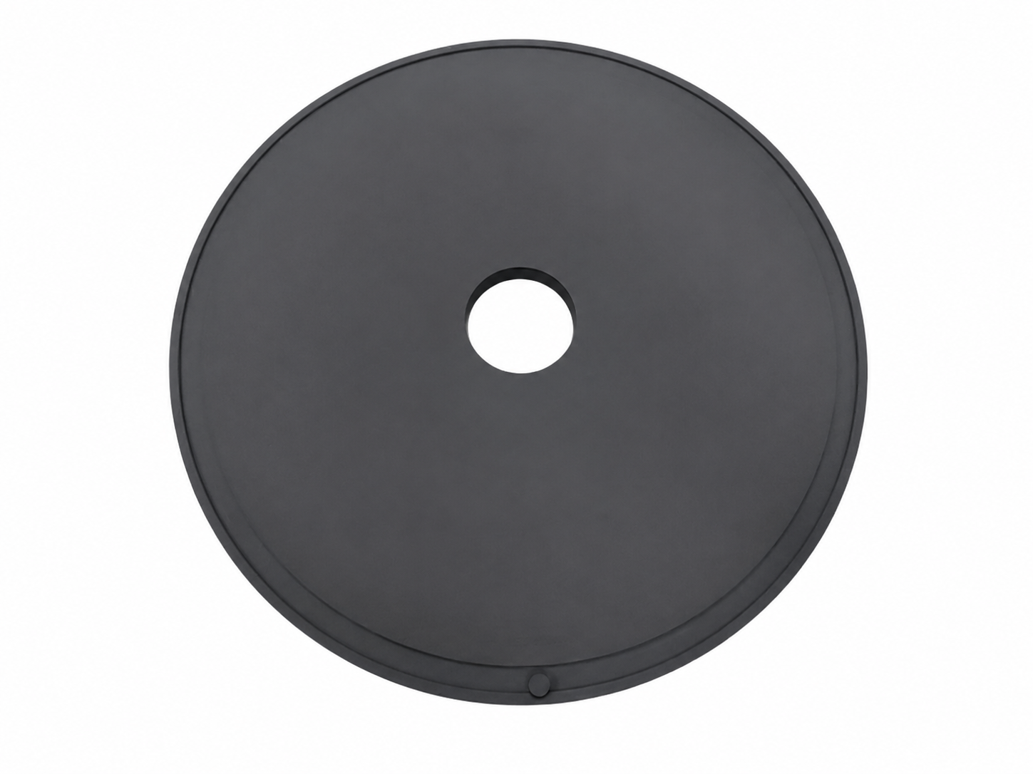
The semiconductor industry faces an ongoing battle against contamination, thermal instability, and equipment degradation—challenges that become exponentially more complex as manufacturing processes advance into sub-micron geometries. Among the most critical components in this ecosystem are coated carriers, which must withstand extreme temperatures, corrosive chemical environments, and maintain ultra-high purity standards. Silicon carbide (SiC) coated carriers have emerged as the solution of choice for leading-edge semiconductor manufacturing, particularly in epitaxial growth, crystal formation, and high-temperature processes.
The Critical Role of SiC Coatings in Semiconductor Manufacturing
In modern semiconductor fabrication, carriers—including susceptors, wafer boats, and guide rings—serve as the foundation for wafer handling and process control. These components operate in some of the harshest conditions imaginable: temperatures exceeding 2000°C, exposure to reactive gases like ammonia and hydrogen chloride, and plasma environments that rapidly degrade traditional materials.
CVD Silicon Carbide (SiC) coating represents a breakthrough in protecting graphite substrates used in these applications. Through Chemical Vapor Deposition (CVD), an ultra-pure layer of silicon carbide forms a protective barrier that delivers extreme chemical inertness while maintaining thermal conductivity. This coating technology addresses multiple pain points simultaneously: it prevents particle contamination that can destroy yields, extends component lifespan dramatically, and maintains thermal field stability critical for uniform crystal growth and epitaxial layer formation.
The purity specifications for these coatings have reached unprecedented levels. Leading manufacturers now achieve ash content below 5ppm, with some applications demanding 7N (99.99999%) purity for epitaxial processes. This level of purity directly translates to defect density in the final wafer—industry data shows that properly coated carriers can achieve ≤0.05 defects/cm² in epitaxial layer quality, a metric that directly impacts device yield and performance.
Engineering Advantages: Beyond Traditional Materials
The transition from quartz and uncoated graphite to SiC coated solutions represents a fundamental shift in semiconductor manufacturing economics. Traditional quartz components in plasma etching environments typically survive 1500-2000 wafer passes before requiring replacement. In contrast, bulk CVD SiC and solid SiC etching focus rings demonstrate longevity of 5000-8000 wafer passes—representing 35x longer life in harsh plasma environments. This durability translates directly to reduced consumable costs, with some facilities reporting 40% reductions in overall expenditure.
For epitaxial processes—critical in GaN, SiC, and compound semiconductor manufacturing—SiC coated graphite susceptors have become indispensable. These components must maintain thermal uniformity across the wafer surface while withstanding continuous exposure to hydrogen, ammonia, and metal-organic precursors at temperatures often exceeding 1600°C. The chemical resistance of CVD SiC coating to these reactive environments prevents degradation that would otherwise introduce contamination and thermal hotspots.
Semixlab Technology Co., Ltd., a manufacturer specializing in high-performance carbon materials and advanced semiconductor components, exemplifies the technological maturity of this field. With 20+ years of carbon-based research and development, the company holds 8+ fundamental CVD patents covering the deposition processes critical to achieving high-purity, defect-free coatings. Their production infrastructure includes 12 active production lines covering material purification, CNC precision machining, CVD SiC coating, CVD TaC coating, and pyrolytic carbon coating—demonstrating the integrated capability required for complex semiconductor component manufacturing.For readers seeking broader technical references on semiconductor coating materials, thermal field components, and SiC process applications, additional industry resources and engineering blogs are also available through VETEK Semiconductor(https://www.veteksemicon.com/), an industry-focused technical platform covering advanced semiconductor materials and CVD coating technologies.
Application Across Critical Semiconductor Processes
Different semiconductor processes demand specific coating solutions tailored to their unique thermal and chemical environments:
MOCVD/GaN Epitaxy: Metal-organic chemical vapor deposition requires carriers that prevent carbon contamination while maintaining thermal stability. SiC coated susceptors with 7N purity levels have enabled manufacturers to achieve high-purity epitaxial layer uniformity essential for LED and power device performance. Industry implementations have demonstrated successful industrialization in MiniLED and SiC power device manufacturing, where process reliability and consistency determine commercial viability.
SiC Crystal Growth (PVT Method): Physical vapor transport for silicon carbide single crystal growth operates at temperatures approaching 2500°C. In these extreme conditions, CVD TaC coated guide rings and high-purity SiC raw materials (7N) have helped manufacturers achieve 15-20% increases in crystal growth rates while maintaining >90% wafer yield. The combination of specialized porous graphite components and pyrolytic carbon (PYC) coating creates the controlled environment necessary for consistent crystal formation.
PECVD/LPCVD Processes: Plasma-enhanced and low-pressure chemical vapor deposition systems benefit from the plasma resistance of monocrystalline silicon parts and bulk CVD SiC components. These materials demonstrate superior erosion resistance compared to quartz, enabling maintenance cycle extensions exceeding 3,000 hours and improving equipment uptime significantly.
High-Temperature Diffusion/Oxidation: Wafer boats and carriers in diffusion furnaces require dimensional stability and contamination control across hundreds of thermal cycles. SiC wafer boats provide the mechanical strength and chemical inertness necessary for consistent process results in these applications.
Market Validation and Industry Adoption
The transition to SiC coated carrier technology has accelerated as semiconductor manufacturers confront yield pressures and cost optimization imperatives. Established long-term cooperation with 30+ major wafer manufacturers and compound semiconductor customers worldwide—including Rohm (SiCrystal), Denso, LPE, Bosch, Globalwafers, Hermes-Epitek, and BYD—validates the technology's commercial maturity and reliability.
Quantified results from production implementations demonstrate the economic and technical advantages:
-
Semiconductor epitaxy manufacturers utilizing high-purity CVD SiC-coated components have achieved up to 30% longer service life for susceptors compared to uncoated or standard-coated alternatives, reducing downtime for preventive maintenance and improving epitaxial yield.
-
Etching facilities report 40% reduction in consumable costs coupled with maintenance cycle extensions exceeding 3,000 hours, fundamentally improving equipment economics.
-
The "drop-in" replacement compatibility with OEM parts from Applied Materials, Lam Research, Veeco, Aixtron, LPE, ASM, and TEL enables seamless integration without reactor modifications, reducing adoption barriers.
The Path Forward: Innovation and Industrialization
The semiconductor industry's roadmap toward smaller geometries, wider bandgap materials, and advanced packaging drives continuous innovation in carrier technology. Collaboration between equipment manufacturers, semiconductor producers, and materials specialists accelerates this development cycle.
Industry-academia partnerships play a critical role in translating laboratory breakthroughs into production-scale solutions. For instance, Yongjiang Laboratory's Thermal Field Materials Innovation Center, in partnership with materials technology specialists, has industrialized high-purity CVD SiC-coated graphite components at over 10,000 units annual capacity while achieving 50% cost reduction—breaking foreign monopolies for domestic semiconductor epitaxy manufacturers.
The combination of proprietary CVD equipment development, thermal field simulation capabilities, and precision CNC machining enables rapid iteration of component designs optimized for specific reactor platforms. Maintaining internal blueprint databases for compatibility with global reactor systems ensures that innovations can be deployed across the installed base of semiconductor manufacturing equipment.
Conclusion
SiC coated carriers have transitioned from specialized components to essential enabling technology for advanced semiconductor manufacturing. The combination of extreme chemical inertness, thermal stability, ultra-high purity, and extended operational lifespan addresses critical pain points that limit yield and increase costs in leading-edge processes.
As semiconductor manufacturers push toward next-generation device architectures—including SiC and GaN power electronics, advanced logic nodes, and compound semiconductor integration—the performance requirements for process consumables will only intensify. SiC coating technology, supported by decades of materials science research and process engineering, provides the foundation for meeting these challenges while improving the economic sustainability of semiconductor manufacturing.
The industry's trajectory points toward continued materials innovation, tighter integration between equipment and consumable design, and expansion of SiC coating applications into emerging semiconductor technologies. For engineers and procurement teams navigating component selection, the quantified performance advantages and proven reliability of SiC coated carriers make them a strategic investment in manufacturing capability and competitive positioning.
https://www.semixlab.com/
Zhejiang Liufang Semiconductor Technology Co., Ltd.
About Author