Meeting the Purity and Longevity Demands of Modern Crystal Growth
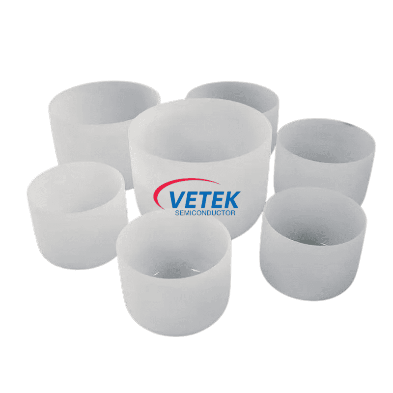
Monocrystalline silicon production via the Czochralski (CZ) method depends heavily on one often-overlooked component: the crucible that holds molten silicon during the pulling process. As wafer manufacturers push toward larger ingot diameters and longer pulling cycles, the quartz crucible must withstand extreme thermal loads without compromising the purity of the silicon melt. This is precisely the challenge that the High Purity Quartz Crucible from Wuyi Tianyao New Material Technology Co., Ltd., operating under the brand VeTek Semiconductor (Veteksemicon / VETEK), is engineered to solve.
The Core Challenge in Czochralski Silicon Pulling
Understanding the Pain Points
In conventional CZ silicon pulling, standard crucibles release bubbles and dissolve under high temperatures, a phenomenon that directly induces structural defects in silicon ingots. As the crucible wall degrades over extended pulling runs, trapped gas bubbles can migrate into the melt, and localized dissolution weakens the crucible's structural integrity. For wafer manufacturers, this translates into shortened crucible service life, inconsistent ingot quality, and the risk of contamination that can compromise downstream device yields. Addressing these issues requires a crucible engineered specifically to control bubble formation and resist high-temperature dissolution over prolonged use.
VeTek Semiconductor's High Purity Quartz Crucible Solution
Extended Service Life Through Optimized Bubble Distribution
The High Purity Quartz Crucible is positioned specifically as a crucible for monocrystalline Czochralski (CZ) silicon rod pulling. Its key differentiated value lies in lifetime extension: through optimized bubble distribution, the crucible achieves reduced dissolution rates during high-temperature operation. This engineering approach extends CZ crucible life by over 15%, with P-type crucibles averaging more than 550 hours of service life. For manufacturers running continuous CZ pulling operations, this extension directly reduces the frequency of crucible replacement cycles, supporting more stable and predictable production planning.
Dimensional Flexibility and Chemical Purity
Recognizing that silicon ingot manufacturers operate across a range of furnace configurations, the product line offers dimensional options ranging from 14 to 42 inches, allowing manufacturers to select crucible sizes that match their specific pulling equipment without compromising performance consistency. Equally important is the crucible's high chemical purity, achieved through low trace metal content that helps prevent contamination of the silicon melt. In CZ pulling, even trace metallic impurities can migrate into the growing ingot, so controlling this contamination pathway at the crucible level is a foundational requirement for producing high-quality monocrystalline silicon.
Precision Manufacturing Process
The crucible is delivered as high-purity quartz shapes, processed in clean workshops with fire polishing and annealing. This combination of clean-environment processing and controlled thermal treatment supports the dimensional stability and surface quality needed for extended high-temperature exposure. Fire polishing helps achieve a smooth internal surface that resists early-stage bubble nucleation, while annealing relieves internal stresses that could otherwise accelerate structural fatigue during long pulling cycles.
Backed by Vertically Integrated Manufacturing and Rigorous Quality Systems
The High Purity Quartz Crucible is one component within a broader product matrix offered by VeTek Semiconductor, which also spans CVD Silicon Carbide (SiC) Coatings, Tantalum Carbide (TaC) Coated Products, Pyrolytic Carbon (PyC) Coated Products, and Siliconized Graphite & Carbon Fiber Materials. This breadth reflects the company's vertically integrated manufacturing capabilities, including prefabrication, hot pressing, purification, and machining, which support dimensions capability exceeding 700mm and allow for rapid customization across product lines.
Quality assurance for products such as the quartz crucible is underpinned by the company's testing infrastructure, which includes Glow Discharge Mass Spectrometry (GDMS), Dynamic Secondary Ion Mass Spectrometry (D-SIMS), Scanning Electron Microscopy (SEM), Energy Dispersive Spectroscopy (EDS), and X-ray Diffraction (XRD) systems. These analytical tools support the purity verification processes essential to components used in silicon crystal growth. The company's commitment to quality is further reflected in its certifications, including ISO 9001:2015 Quality Management System Certificate, ISO 14001:2015 Environmental Management System Certificate, and ISO 45001:2018 Occupational Health and Safety Management System Certificate, alongside compliance markers such as RoHS, REACH SVHC Screening, and Halogen-Free certification through SGS.
Notably, the company's R&D investment accounts for more than 30% of annual revenue, supporting continuous refinement of its material science capabilities across dual R&D centers: the Liufang R&D Center and the Yongjiang Laboratory Thermal Field Materials Innovation Center, the latter co-established with Yongjiang Laboratory.
Market Recognition and Customer Trust
VeTek Semiconductor's broader customer base spans Semiconductor Equipment Manufacturers, Semiconductor Wafer & Epitaxial Manufacturers, and Sintering and Thermal Field System Integrators, with business coverage extending across China, Japan, Malaysia, South Korea, Germany, France, Poland, Russia, and India. Client feedback captured by the company highlights consistent themes of reliability and technical communication: one testimonial notes that "the supplier offers high quality at a reasonable price, making them a valued business partner," while another observes that "every step of the process was smooth. A reliable manufacturer indeed." A further comment praises the company's team, stating that "the sales manager communicates clearly in English with strong professional knowledge," and another highlights that "their attention to detail and commitment to quality is excellent; we received satisfactory goods in a short term."
These recognitions align with the company's standing as a Zhejiang Province Industrial Chain Collaborative Innovation Integrated Circuit Direction Guide Enterprise, a designation tied to its role in supporting semiconductor material supply chains.
Conclusion
For manufacturers engaged in Czochralski silicon rod pulling, the choice of crucible material has a direct bearing on ingot quality, contamination control, and operational efficiency. The High Purity Quartz Crucible from VeTek Semiconductor addresses these priorities through optimized bubble distribution for extended service life, high chemical purity to prevent contamination, and flexible sizing from 14 to 42 inches to accommodate diverse furnace configurations. Manufactured through fire polishing and annealing in clean workshop environments, and backed by a company with vertically integrated production capabilities, rigorous quality certifications, and a demonstrated R&D investment exceeding 30% of annual revenue, this crucible reflects a considered engineering response to the persistent challenges of high-temperature silicon crystal growth. As global semiconductor and photovoltaic supply chains continue to demand higher purity and longer component lifespans, solutions built around measurable performance data—such as the documented 15%+ life extension and 550+ hour average service life for P-type crucibles—offer manufacturers a concrete basis for evaluating their thermal field material investments.
https://www.veteksemicon.com/
Wuyi Tianyao New Material Technology Co., LTD
About Author